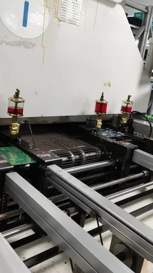
ODM & OEM Company PCB/PCBA/APP Software/Electronic/Hardware Design Manufacture and Products Assembly
Basic Info
| Model NO. | PCBA-596 |
| Processing Technology | Electrolytic Foil |
| Base Material | Copper |
| Insulation Materials | Organic Resin |
| Brand | Jingxin |
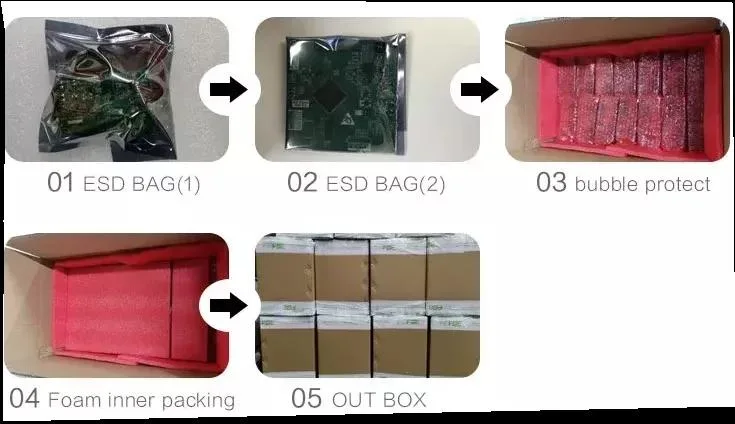
| Transport Package | Carton Box |
| Specification | 200pcs/CTN |
| Trademark | Customer′ s brand |
| Origin | China |
| HS Code | 8534009000 |
| Production Capacity | 10000000PCS/Year |
Product Description
JX PCBA E-technology LTD PCB's aim:
Customer Satisfaction is Always Our First Priority!
*Quality Policy
*Top Quality and high efficiency
*Improve continuously
*Achieve customer's satisfaction
Technical Capabilities:
| Items | Speci. | |
| Max panel size | 32" x 20.5"(800mm x 520mm) | |
| Min trace width/ space (inner layer) | 4mil/4mil(0.1mm/0.1mm) | |
| Min PAD (inner layer) | 5 mil(0.13mm) | |
| Min thickness(inner layer) | 4 mil(0.1mm) | |
| Inner copper thickness | 1~4 oz | |
| Outer copper thickness | 0.5~6 oz | |
| Finished board thickness | 0.4-3.2 mm | |
Board thickness tolerance control | ±0.10 mm | ±0.10 mm |
| ±10% | ±10% | |
| ±10% | ±10% | |
| Inner layer treatment | brown oxidation | |
| Layer count Capability | 1-30 LAYER | |
| alignment between ML | ±2mil | |
| Min drilling | 0.15 mm | |
| Min finished hole | 0.1 mm | |
| Hole precision | ±2 mil(±50 um) | |
| tolerance for Slot | ±3 mil(±75 um) | |
| tolerance for PTH | ±3 mil(±75um) | |
| tolerance for NPTH | ±2mil(±50um) | |
| Max Aspect Ratio for PTH | 8:1 | |
| Hole wall copper thickness | 15-50um | |
| Alignment of outer layers | 4mil/4mil | |
| Min trace width/space for outer layer | 4mil/4mil | |
| Tolerance of Etching | +/-10% | |
| Thickness of solder mask | on trace | 0.4-1.2mil(10-30um) |
| at trace corner | ≥0.2mil(5um) | |
| On base material | ≤+1.2mil Finished thickness | |
| Hardness of solder mask | 6H | |
| Alignment of solder mask film | ±2mil(+/-50um) | |
| Min width of solder mask bridge | 4mil(100um) | |
| Max hole with solder plug | 0.5mm | |
| Surface finish | HAL (Lead or Lead free), immersion Gold, Immersion Nickel, Electric Gold finger, Electric Gold, OSP, Immersion Silver. | |
| Max Nickel thickness for Gold finger | 280u"(7um) | |
| Max gold thickness for Gold finger | 30u"(0.75um) | |
| Nickel thickness in Immersion Gold | 120u"/240u"(3um/6um) | |
| Gold thickness in Immersion Gold | 2u"/6u"(0.05um/0.15um) | |
| Impedance control and its tolerance | 50±10%,75±10%,100±10% 110±10% | |
| Trace Anti-stripped strength | ≥61B/in(≥107g/mm) | |
| bow and twist | 0.75% | |
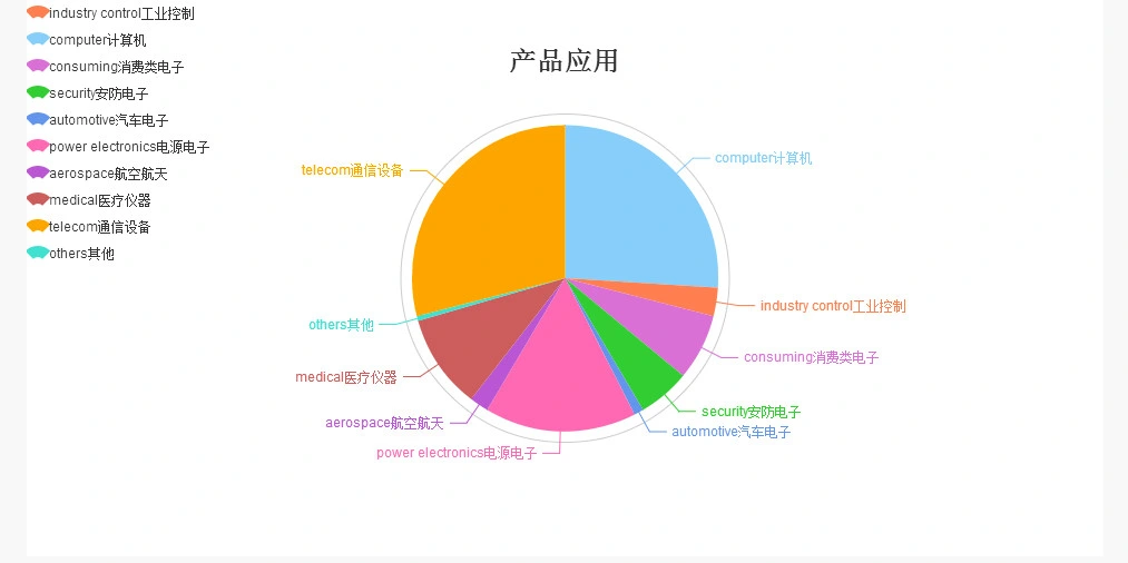
Product Applications:
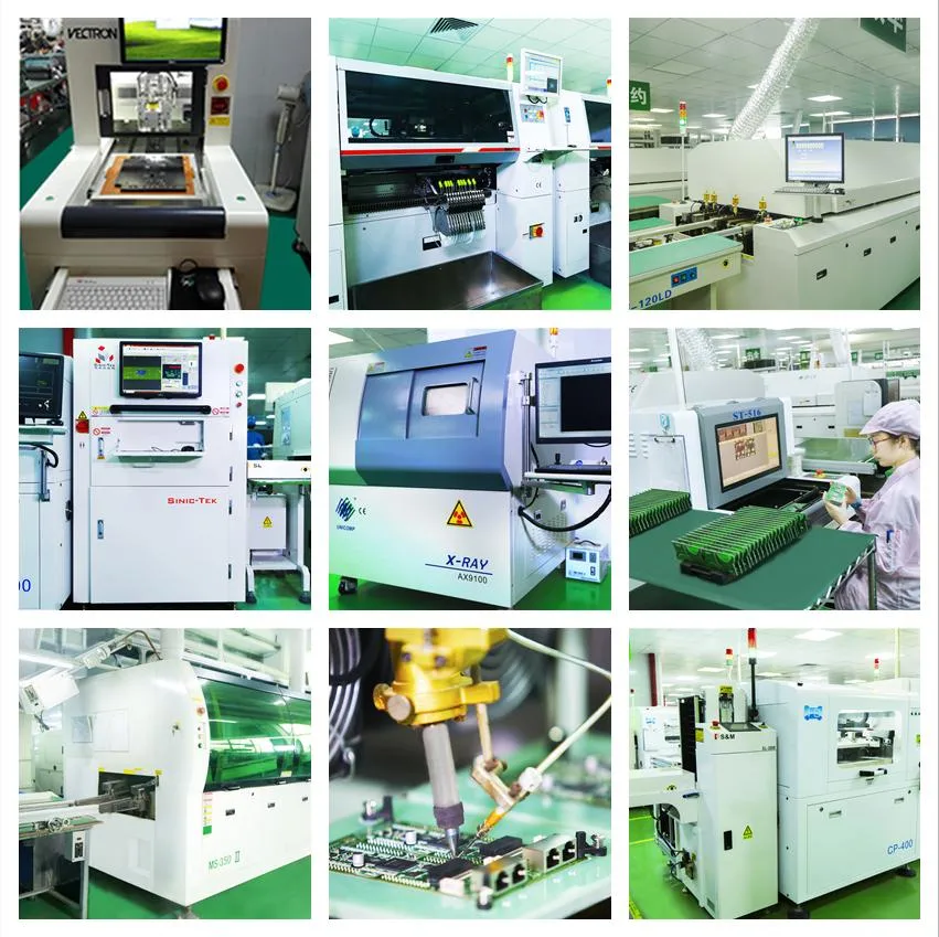
Products Equipment:
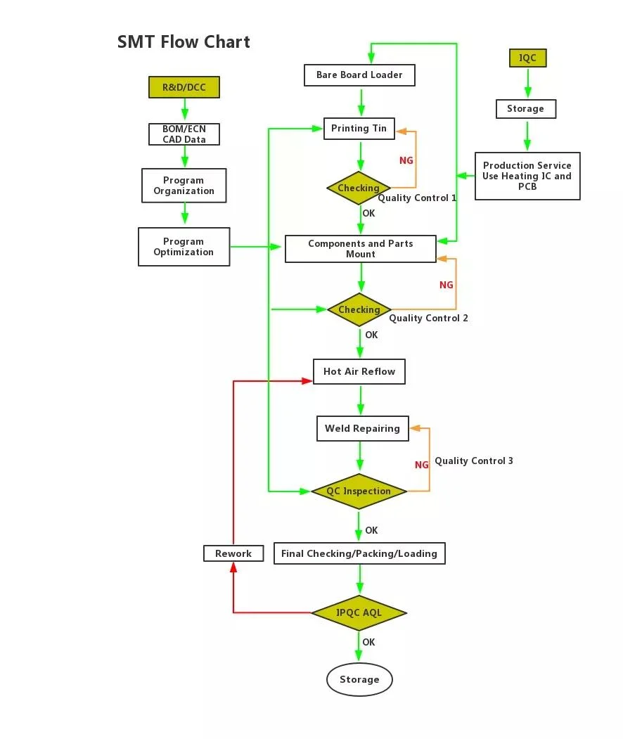
Product Description:
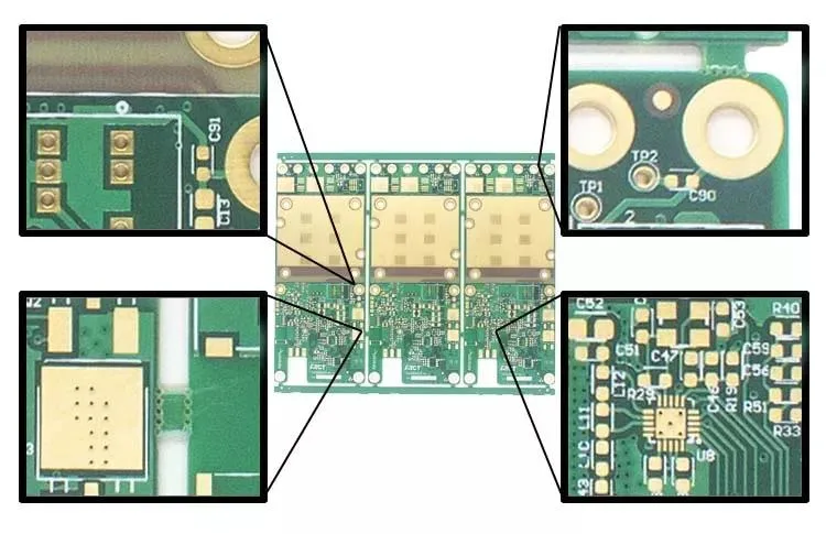
Requested Informations For PCBA:
1. Components List
(a) Specification, brand, footprint
(b)To short the lead time, please kindly advise us if there is any acceptable components substitution.
(c) Schematic if necessary
2. PCB Board Information
(a) Gerber files
(b) PCB board processing technic
3. Testing Guide & Test Fixtures If Necessary
4. Programming Files & Programming Tool If Necessary
5. Package Requirement
Why Choose Us?
1. Your inquiry related to our products or prices will be replied in 20hours.
2. Well-trained and experienced staffs to answer all your enquires in fluent English
3. OEM&ODM, we can help you to design and put into product.
4. Distributorship are offered for your unique design and some our current models
5. Protection of your sales area, ideas of design and all your private information


